Table of Contents
TDA2050 amplifier circuit board 32W, The TDA 2050 is a monolithic integrated circuit in Pentawatt package, intended for use as an audio class AB audio amplifier. Thanks to its high power capability the TDA2050 is able to provide up to 35W true rms power into 4 ohm load @ THD = 10%, VS = ±18V, f = 1KHz and up to 32W into 8 ohm load @ THD = 10%, VS = ±22V, f = 1KHz. Moreover, the TDA 2050 delivers typically 50W music power into 4 ohm load over 1 sec at VS=
22.5V, f = 1KHz.
The high power and very low harmonic and crossover distortion (THD = 0.05% typ, @ VS = ±22V, PO = 0.1 to 15W, RL=8ohm, f = 100Hz to 15KHz) make the device most suitable for both HiFi and high class TV sets.
- High output power
- (50w music power IEC 268.3 rules)
- High operating supply voltage (50v)
- Single or split supply operations
- Very low distortion
- Short circuit protection (out to Gnd)
- Thermal shutdown
SHORT CIRCUIT PROTECTION
The TDA 2050 has an original circuit which limits the current of the output transistors. The maximum output current is a function of the collector emitter voltage; hence, the output transistors work within their safe operating area. This function can therefore be considered as being peak power limiting rather than simple current limiting.
It reduces the possibility that the device gets damaged during an accidental short circuit from AC output to ground.
THERMAL SHUTDOWN
The presence of a thermal limiting circuit offers the following advantages:
1)An overload on the output (even if it is permanent), or an above limit ambient temperature
can be easily tolerated since the Tj cannot be higher than 150 °C.
2)The heatsink can have a smaller factor of safety compared with that of a conventional circuit. There is no possibility of device damage due to high junction temperature. If for
any reason, the junction temperature increases up to 150 °C, the thermal shutdown simply reduces the power dissipation and the current consumption.
Schematic of Amplifier with TDA2050

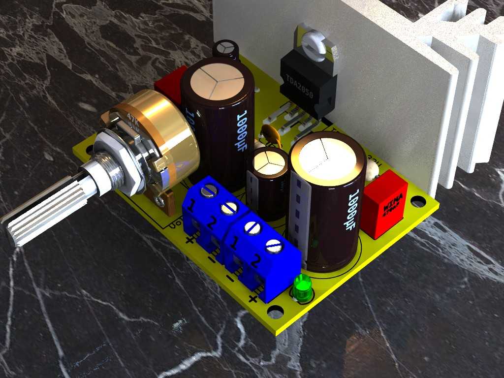
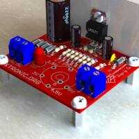
Suggested PCB for TDA2050 Amp


BOM to assemble the power amplifier.
Last update: 08/08/2021 23:32
| Part | Value | Description | Quantity |
| Capacitors | |||
| C1 | 2.2µF | Ceramic Capacitor | 1 |
| C2 | 100µF | Electrolytic capacitor | 1 |
| C3, C7 | 1000µF | Electrolytic capacitor | 2 |
| C4 | 22µF | Electrolytic capacitor | 1 |
| C5 | 100nF | Ceramic Capacitor | 1 |
| C6 | 470nF | Ceramic Capacitor | 1 |
| Semiconductors | |||
| IC1 | TDA2050 | Audio amplifier integrated circuit | 1 |
| LED1 | led 3 mm | 3MM LED any color | 1 |
| Resistors 1/4W 5% | |||
| R1, R2, R3, R5 | 22k | Red, Red, Orange, Gold | 4 |
| R4 | 680 | Blue, Gray, Brown, Gold | 1 |
| R6 | 2.2/2W | Red, Red, Gold, Gold | 1 |
| R7 | 10k | Brown, Black, Orange, Gold | 1 |
| Miscellaneous | |||
| CN1 | IN | 2.54 mm 2-Way Connector | 1 |
| CN2 | DC | Terminal block 2 pin 5.08 mm | 1 |
| CN3 | OUT | Terminal block 2 pin 5.08 mm | 1 |
| P1 | 47K (473) | Potentiometer 47K | 1 |
| Solder, Wire, PCB, Box, power supply | |||
The source for this circuit should be 12 to 45 volts/ 2 amps*.
It requires a heat sink and the source must be DC voltage. You can use notebook sources that looks cool.
* If you use a source higher than 25V the electrolytic must have a working voltage of 50V and if > 40 Volts they must be 63 Volts!
Download the files for this assembly version 2021 – updated files with board in PNG, PDF, Gerber and postscript formats.
This IC can be found for sale in the market as TDA2050TB, TDA2050L, TDA2050V and TDA2050A
Buy TDA2050 in Aliexpress with free Shipping in the Worldwide.


Ola Toni Pode resistores de 1/2w
Olá Cardoso
Pode sim.
Alguien pudo hacer pcb para capacitores de 50v? El diseño presente es para capacitores más chicos
This TDA2050 circuit is working & sound quality is better than others. Thanks Mr. Toni.
Hello Md. Masudur Rahman
Thanks your feedback!
Funciona con 12v fuente de Pc tambien?
Hola Cristian
Si, funciona!
Thanks for the circuit…100% working
what is the size of board TDA 2050?
Tell me who made this successfully
Hello kamlesh
This is a single circuit!
What type of font are you using?
Voltage and current
Guys please tell me that is it working amplifier or not
HI kamlesh
Its work!
What is the voltage of all capacitor pls.
El condensador C7 esta al reves.
ya tu sabee broouu
tengo un problema, despues de funcionar unos segundos me revienta el capacitor de salida de audio.
can u pls tell me that c5 capacitor is of 100nf is it 25v, 63v, or 100v
Hello Aman
Power supply < 18V = Capacitors 25V Power supply < 25V = Capacitors 35V Power supply < 40V = Capacitors 50V Power supply 40 at 45V = Capacitors 63V
saya pernah bikin power amplifier sub TDA 7294.tapi kok suaranya kecil banget.bassnya gak bisa keluar.
saya dari Indonesia.thank
Comment:
saya tahu..dalam pemasangan part ada yang salah sehingga gain tidak keluar suara,
cek polaritas part anda, jangan sampai terbalik
to choleke kenter
You actually make it seem so easy with your presentation but
I find this matter to be really something that I think I
would never understand. It seems too complicated and extremely broad for me.
I am looking forward for your next post, I’ll try to get the hang of it!
2050ic PCB and valiv apart
hi ! am a starter in electronic field.i really appreciate what you are doing.
Aló Toni please envíame el PCB de este amplicador. Muito brigado!
Hola Toni por favor me puedes enviar el PCB de este amplificador. Muchas gracias.
Hi, i bnuilded it and it don’t works and i don’t know why. PCB is clean, pins are ok and as supply i’m using 24v old notebook power supply. I can’t hear anything in the speaker. TDA or any differnt component don’t heat. At first start i added fuse 3,5A and it doesnt blow so theres not problem. Can you help me please??
I fixed it!! There is a mystake on PCB…
TDA pins are inverted.
Hello to all who come to this page to build your audio amplifier. I have tested this circuit. and let me tell you that is a mistake. The PCB is in no way mirror. printed as well, to work, the TDA2050 I will have to put on the side of the tracks. and to prove it, see the datasheet of the TDA2050. In the Pin1 is the audio input. And when they finish the PCB is in Vs Pin1 +.
Luck …
ohh please its fine flip the image so that u can read the pcb words correctly i.e the +ve and -ve and xtronic read correctly and there u go…………use paints to flip the image horrizontally then rotate +180……..good luck
Hola a todos los que lleguen a esta página para construir su amplificador de audio. Lo he probado a este circuito. y dejenme decirle que tiene un error. El PCB no está en modo espejo. si lo imprimen así, para que funcione, el TDA2050 lo tendrán que poner del lado de las pistas. y para corroborarlo, vean el datasheet del TDA2050. En el Pin1 va la entrada de audio. Y cuando terminen el PCB, el Pin1 queda en Vs+.
Suerte…
Can you send me the PDF files of the pcb? Thank you!
Please send me PDF files of the PCB I want to try this :)
[email protected]
Tnx and greetings from Serbia
:)
please send me a power supply circuit for this amplifier
Read more: Circuit 32w hi-fi audio power amplifier – TDA2050 | Xtronic Free Electronic Circuits and Informations http://xtronic.org/circuit/amplifier/32w-hi-fi-power-amplifier-tda2050/#ixzz22NI7YK1d
Hola capo muy bueno una pregunta funciona con 12vcc? me podes mandar al correo el PCB para imprimir? gracias muy bueno!!!!!
so fico um pouco em duvida sobre o capacitor 0,47uf ele por acaso é igual a 47pf, mas o progeto é muito bom.
0.47uF = 47nF
HEllo Mr Tony can you send me PCB layout and Shematic for TDA 2050 Brridge Amp thanks
PLEASE!
hello! can you send me a power supply pcb layout for this amplifier coz i wanna try this circuit.
please send me a power supply circuit for this amplifier.
do you have 18v ps circuit?
Thank you for the PCB layout of single supply!
Ok Alessandro
Good luck