Table of Contents
Circuit diagram tpa3116d2 amplifier board Mini audio amplifier circuit with tpa3116 bridged IC for 100W power with anti-pop. We use the tpa3116d2 IC as a class D audio amplifier and the XL6019 Boost voltage regulator from Xlsemi. Thus, raising the voltage will get the most out of the tpa3116d2 chip.
About the tpa3116 and XL6019 100W mini amplifier circuit
The TPA31xxD2 series are stereo efficient, digital amplifier power stage for driving speakers up to 100 W / 2 Ω in mono. The high efficiency of the TPA3130D2 allows it to do 2 × 15 W without external heat sink on a single layer PCB. The TPA3118D2 can even run 2 × 30 W / 8 Ω without heat sink on a dual layer PCB. If even higher power is needed, the TPA3116D2 does 2 × 50 W / 4 Ω with a small heat-sink attached to its top side PowerPAD. All three devices share the same footprint, enabling a single PCB to be used across different power levels.
The TPA31xxD2 advanced oscillator/PLL circuit employs a multiple switching frequency option to avoid AM interferences; this is achieved together with an option of either master or slave option, making it possible to synchronize multiple devices.
The TPA31xxD2 devices are fully protected against faults with short-circuit protection and thermal protection as well as overvoltage, under voltage, and DC protection. Faults are reported back to the processor to prevent devices from being damaged during overload conditions.
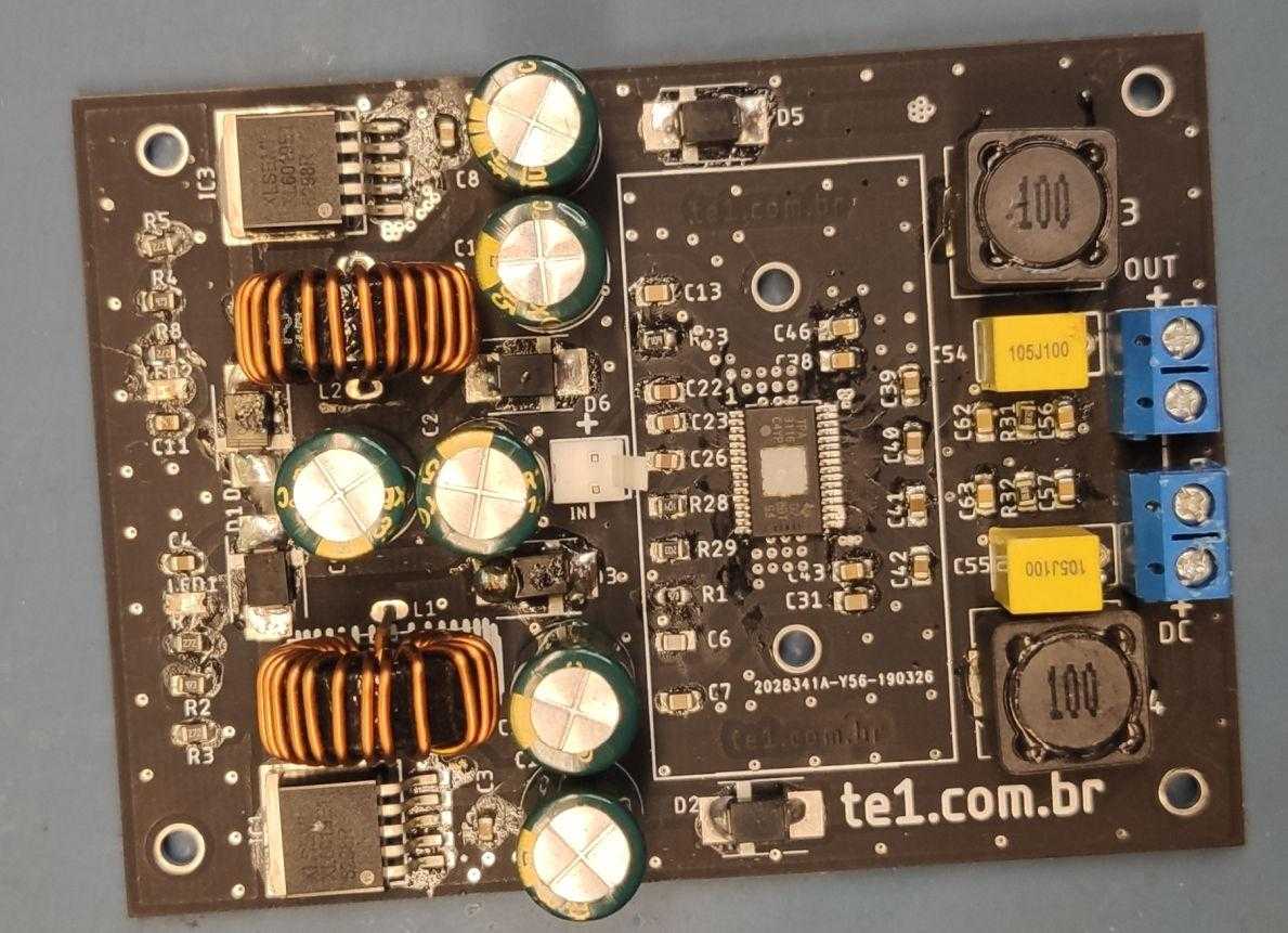
In our application we used the TPA3116D2 IC, configured the oscillator for 400KHz, and added an anti-pop circuit that acts on the mute pin when turning the amplifier on and off, thus avoiding popping when turning the amplifier on and off. The inductors can be SMD or PTH type, as long as they are of 5A or more.
We used 2 XL6019 voltage regulators from Xlsemi that work at 180KHz and can work with up to 5A of current, as we used 2, theoretically up to 10A of current. Sufficient for our amplifier. It is one with the ability to adjust the output voltage by acting on the FB pin. The formula to calculate the output voltage is VOUT=1.25*(1+R2/R1), in our case we have about 23V at the output of our DC/DC converter. This is enough for our TPA3116 chip to work at maximum power. You should add a heat sink to the XL6019 ICs, for this use thermal glue.
SS54 diodes for 5A and 40V or equivalent isolate the supply from each other. At the output of the DC/DC Converter, use good quality electrolytic capacitors.
As we are working with our amplifier for maximum power, we should equip the chip with a heat sink.
It is possible to order this board assembled with the components from JLCPCB or those you prefer, to save money you may be interested in ordering only the basic type components.
Circuit diagram schematic tpa3116d2 amplifier board

Suggested PCB printed circuit board for mounting the amplifier


See other projects with this chip:
- New TPA3118 TPA3116 TPA3130 Stereo Class D Amplifier BTL
- TPA3116d2 amplifier board circuit diagram bridge
You may also like:
- TDA8954 high power Class-D amplifier board 420W
- Circuit custom power supply for audio amplifier Symmetrical
BOM for assembling the amplifier
Last update: 08/02/2022 17:15
| Part | Value | Description | Quantity |
| Resistors | |||
| R1, R2, R4 | 47k (473) | Resistor SMD 0805 | 3 |
| R3, R5 | 2.7K (272) | Resistor SMD 0805 | 2 |
| R7, R8 | 2K (202) | Resistor SMD 0805 | 2 |
| R10, R16 | 470K (474) | Resistor SMD 0805 | 2 |
| R23, R28 | 100K (104) | Resistor SMD 0805 | 2 |
| R29 | 20K (203) | Resistor SMD 0805 | 1 |
| R31, R32 | 3,3 (3R3) | Resistor SMD 0805 | 2 |
| Capacitors | |||
| C1, C2, C5, C8, C9, C12 | 470µ/35 | Electrolytic capacitor | 6 |
| C3, C4, C10, C11, C22, C23, C25, C26, C54, C55 | 1uF | SMD 0805 Ceramic Capacitor | 10 |
| C6 | 47p | SMD 0805 Ceramic Capacitor | 1 |
| C7, C13, C62, C63 | 10n | SMD 0805 Ceramic Capacitor | 4 |
| C27 | 100µ | Electrolytic capacitor | 1 |
| C31, C46 | 100n | SMD 0805 Ceramic Capacitor | 2 |
| C38, C43, C56, C57 | 1n | SMD 0805 Ceramic Capacitor | 4 |
| C39, C40, C41, C42 | 220n | SMD 0805 Ceramic Capacitor | 4 |
| Semiconductors | |||
| D1, D2, D3, D4, D5, D6 | SS54 | Schottky diode SMC | 6 |
| D7, D8 | 1n4148 | Diode SOD80C | 2 |
| LED1, LED2 | LED red | LED SMD 0805 | 2 |
| IC1, IC3 | XL6019 | 5A Switching Current Boost DC/DC Converter TO263-5L | 2 |
| IC2 | TPA3116d2DADR | DAD32 Class D Audio Amplifier | 1 |
| Q1 | PMBT3906 | Transistor PNP SMD SOT23-3 | 1 |
| Miscellaneous | |||
| L1, L2 | 47uH 5A | Toroidal Inductor | 2 |
| L3, L4 | 10uH | Inductor SMD CDR127 (optional) | 2 |
| DC | Alimentação | Terminal block 2 pin 5.08 mm. | 1 |
| IN | Audio Input | Terminal block 2 pin 5.08 mm. | 1 |
| OUT | Audio Output | Terminal block 2 pin 5.08 mm. | 1 |
| Solder, Wires, PCB, case, font, heatsink, etc. | |||
Download files of this assembly, including PCB board in Gerber, PNG, PDF format.
- Datasheet em PDF do CI tpa3116d2 — Texas Instruments
- Datasheet em PDF do CI XL6019 — Xlsemi
- Datasheet em PDF do diodo Schottky


Hi,
please upload the gerber files. I am not able to download the files. link?
Good amplifier . But how’s the noise when playing some music ?