TPA3116 TPA3118 and TPA318 and TPA3130 BTL Class D Stereo Power Amplifier with 15+ 15W, 30 + 30W or 50 + 50W power supply of 4.5 to 26V with analog input. The TPA31XXD2 chip series are an efficient amplifier with digital power stage for power up to 100W in the mono version. The high efficiency of CI’s TPA3116 TPA3118 and TPA3130 make it widely used on portable devices such as mini portable boxes such as JBL CHARGE 3 (TPA3118D2) and HARMAN KARDON ONYX STUDIO (TPA3116D2) and can be powered by batteries.
TPA31xxd2 features an advanced PLL oscillator circuit with multiple switching switching frequencies to avoid interference in AM. This also together with
The master or slave option, making it possible to synchronize multiple devices.
The TPA31xxD2 series are stereo efficient, digital amplifier power stage for driving speakers up to 100 W / 2 Ω in mono. The high efficiency of the TPA3130D2 allows it to do 2 × 15 W without external heat sink on a single layer PCB. The TPA3118D2 can even run 2 × 30 W / 8 Ω without heat sink on a dual
layer PCB. If even higher power is needed the TPA3116D2 does 2 × 50 W / 4 Ω with a small heatsink attached to its top side PowerPAD. All three devices share the same footprint enabling a single
PCB to be used across different power levels. The TPA31xxD2 advanced oscillator/PLL circuit employs a multiple switching frequency option to avoid AM interferences; this is achieved together with an option of either master or slave option, making it possible to synchronize multiple devices. The TPA31xxD2 devices are fully protected against faults with short-circuit protection and thermal protection as well as overvoltage, undervoltage, and DC protection. Faults are reported back to the processor to prevent devices from being damaged during overload conditions.

TPA3116 TPA31130 TPA3130 chips are fully protected against failures, with short circuit protection, thermal protection, overvoltage, undervoltage and DC protection. Failures are reported back to the processor to prevent devices from being damaged during overload conditions.
Function Detail Pins TPA3116D2, TPA3118D2 and TPA3130D2
| Pin | TYPE¹ | DESCRIPTION | |
| Nº | NAME | ||
| 1 | MODSEL | I | Mode selection logic input (LOW = BD mode, HIGH = 1 SPW mode). TTL logic levels with compliance to AVCC. |
| 2 | SDZ | I | Shutdown logic input for audio amp (LOW = outputs Hi-Z, HIGH = outputs enabled). TTL logic levels with compliance to AVCC. |
| 3 | FAULTZ | DO | General fault reporting including Over-temp, DC Detect. Open drain. FAULTZ = High, normal operation FAULTZ = Low, fault condition |
| 4 | RINP | I | Positive audio input for right channel. Biased at 3 V. |
| 5 | RINN | I | Negative audio input for right channel. Biased at 3 V. |
| 6 | PLIMIT | I | Power limit level adjust. Connect a resistor divider from GVDD to GND to set power limit. Connect directly to GVDD for no power limit. |
| 7 | GVDD | PO | Internally generated gate voltage supply. Not to be used as a supply or connected to any component other than a 1 µF X7R ceramic decoupling capacitor and the PLIMIT and GAIN/SLV resistor dividers. |
| 8 | GAIN/SLV | I | Selects Gain and selects between Master and Slave mode depending on pin voltage divider. |
| 9 | GND | G | Ground |
| 10 | LINP | I | Positive audio input for left channel. Biased at 3 V. Connect to GND for PBTL mode. |
| 11 | LINN | I | Negative audio input for left channel. Biased at 3 V. Connect to GND for PBTL mode. |
| 12 | MUTE | I | Negative audio input for left channel. Biased at 3 V. Connect to GND for PBTL Mute signal for fast disable/enable of outputs (HIGH = outputs Hi-Z, LOW = outputs enabled). TTL logiclevels with compliance to AVCC.mode. |
| 13 | AM2 | I | AM Avoidance Frequency Selection |
| 14 | AM1 | I | AM Avoidance Frequency Selection |
| 15 | AM0 | I | AM Avoidance Frequency Selection |
| 16 | SYNC | DIO | Clock input/output for synchronizing multiple class-D devices. Direction determined by GAIN/SLV terminal |
| 17 | AVCC | P | Analog Supply |
| 18 | PVCC | P | Power supply |
| 19 | PVCC | P | Power supply |
| 20 | BSNL | BST | Boot strap for negative left channel output, connect to 220 nF X5R, or better ceramic cap to OUTNL |
| 21 | OUTNL | PO | Negative left channel output |
| 22 | GND | G | Ground |
| 23 | OUTPL | PO | Positive left channel output |
| 24 | BSPL | BST | Boot strap for positive left channel output, connect to 220 nF X5R, or better ceramic cap to OUTPL |
| 25 | GND | G | Ground |
| 26 | BSNR | BST | Boot strap for negative right channel output, connect to 220 nF X5R, or better ceramic cap to OUTNR |
| 27 | OUTNR | PO | Negative right channel output |
| 28 | GND | G | Ground |
| 29 | OUTPR | PO | Positive right channel output |
| 30 | BSPR | BST | Boot strap for positive right channel output, connect to 220 nF X5R or better ceramic cap to OUTPR |
| 31 | PVCC | P | Power supply |
| 32 | PVCC | P | Power supply |
| 33 | PowerPAD | G | Connect to GND for best system performance. If not connected to GND, leave floating. |
(1) TYPE: DO = Digital Output, I = Analog Input, G = General Ground, PO = Power Output, BST = Boot Strap.
See our project of amplifiers and power Supply
The TPA31xxD2 device is a highly efficient Class D audio amplifier with integrated 120m Ohms MOSFET that allows output currents up to 7.5 A. The high efficiency allows the amplifier to provide an excellent audio performance without the need for a bulky heat sink.
The device can be configured for either master or slave operation by using the SYNC pin. This helps to prevent audible beats noise
Gain Setting and Master and Slave TPA3116D2, TPA3118D2 or TPA3130D2
The gain of the TPA31xxD2 family is set by the voltage divider connected to the GAIN/SLV control pin. Master or Slave mode is also controlled by the same pin. An internal ADC is used to detect the 8 input states. The first four stages sets the GAIN in Master mode in gains of 20, 26, 32, 36 dB respectively, while the next four stages sets the GAIN in Slave mode in gains of 20, 26, 32, 36 dB respectively. The gain setting is latched during power-up and cannot be changed while device is powered. Table 1 lists the recommended resistor values and the state and gain:
In our application we are using Master Configuration with 26dB gain and 30K input impedance, but if you prefer, you can use another resistor configuration.
| MASTER / SLAVE MODE |
GAIN | R2 (to GND)¹ | R3 (to GVDD)(1) | INPUT IMPEDANCE |
| Master | 20 dB | 5.6 kΩ | OPEN | 60 kΩ |
| Master | 26 dB | 20 kΩ | 100 kΩ | 30 kΩ |
| Master | 32 dB | 39 kΩ | 100 kΩ | 15 kΩ |
| Master | 36 dB | 47 kΩ | 75 kΩ | 9 kΩ |
| Slave | 20 dB | 51 kΩ | 51 kΩ | 60 kΩ |
| Slave | 26 dB | 75 kΩ | 47 kΩ | 30 kΩ |
| Slave | 32 dB | 100 kΩ | 39 kΩ | 15 kΩ |
| Slave | 36 dB | 100 kΩ | 16 kΩ | 9 kΩ |
(1) Resistor tolerance should be 5% or better.
AM Avoidance EMI Reduction TPA3116, TPA3118 or TPA3130 amp
To reduce interference in the AM radio band, the TPA3116D2 has the ability to change the switching frequency via AM<2:0> pins. The recommended frequencies are listed in Table. The fundamental frequency and its second harmonic straddle the AM radio band listed. This eliminates the tones that can be present due to the switching frequency being demodulated by the AM radio.
| US | EUROPEAN | SWITCHING FREQUENCY (kHz) | AM2 | AM1 | AM0 |
| AM FREQUENCY (kHz) | AM FREQUENCY (kHz) | ||||
| 522-540 | |||||
| 540-917 | 540-914 | 500 | 0 | 0 | 1 |
| 917-1125 | 914-1122 | 600 (or 400) | 0 0 |
1 0 |
0 0 |
| 1125-1375 | 1122-1373 | 500 | 0 | 0 | 1 |
| 1375-1547 | 1373-1548 | 600 (or 400) | 0 0 |
1 0 |
0 0 |
| 1547-1700 | 1548-1701 | 600 (or 500) | 0 0 |
1 0 |
0 |
Frequency selection table
You should use the jumpers on the board (AM0, AM1, AM2) for configuration the oscillation frequency between 400 to 1200kHz. If you want to use the 400khz frequency R12, R13 and R14 resistors can be omitted.
| Oscillator frequency | Selection¹ | Frequency Khz |
|---|---|---|
| AM2=0, AM1=0, AM0=0 | 400 | |
| AM2=0, AM1=0, AM0=1 | 500 | |
| AM2=0, AM1=1, AM0=0 | 600 | |
| AM2=0, AM1=1, AM0=1 | 1000 | |
| AM2=1, AM1=0, AM0=0 | 1200 | |
| AM2=1, AM1=0, AM0=1 | Reserved | |
| AM2=1, AM1=1, AM0=0 | ||
| AM2=1, AM1=1, AM0=1 |
(1) 0 equal = closed jumper, 1 = open jumper
See other project using CI TPA3116
Schematic of the class d amplifier

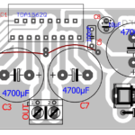
Printed Circuit Board Suggest for Mount AMP Class D


About Amplifier Circuit with chip TPA3116D2, TPA3118D2 or TPA3130D2
You must choose the IC according to your power need, each of a chip will have a maximum power limit. Our circuit is configured for 26dB gain in BTL mode. The coil should be 10uh and at least 5 amps. The circuit around the PMBT3906 transistor is responsible for the MUTE when switching on and off, avoiding the crack in the sound box. The components are SMD 0805, which are not difficult to weld. Also if you prefer you can order the JLCPCB the board already with the soldered SMD components.
Part list List for assembling amplifier with TPA3116
| Parts | Valor | Description | Quantity |
| Capacitors | |||
| C1, C2, C3, C5, C11, C30 | 1uF | Ceramic capacitor SMD 0805 – 25V 10% X7R | 6 |
| C4, C12, C15 | 100n | Ceramic capacitor SMD 0805 – 50V 10% X7R | 3 |
| C6, C7, C8, C9 | 220n | Ceramic capacitor SMD 0805 – 25V 10% X5R | 4 |
| C10, C26, C27, C28, C29 | 10n | Ceramic capacitor SMD 0805 – 100V 10% X7R | 5 |
| C13, C16, C22, C23, C24, C25 | 1n | Ceramic capacitor SMD 0805 – 100V 10% X7R | 6 |
| C14, C17 | 470uF at 1000uF /35V | Electrolytic capacitor | 2 |
| C18, C19, C20, C21 | 680n / 63 or 100V | Capacitor polyester | 4 |
| C31 | 100µ/35V | Electrolytic capacitor | 1 |
| Connectors | |||
| CN1 | INR (Right channel audio input) | Terminal block 2 pin | 1 |
| CN2 | Power (Power 5 to 24V) | Terminal block 2 pin | 1 |
| CN3 | INL (Left channel audio input) | Terminal block 2 pin | 1 |
| CN4 | OUTR (Audio output right channel ) | Terminal block 2 pin | 1 |
| CN5 | OUTL (Audio output left channel ) | Terminal block 2 pin | 1 |
| Semiconductors | |||
| D1, D2 | 1n4148 | SMD diode MiniMELF SOD80 | 2 |
| IC1 | TPA3116D2, TPA3118D2 ou TPA3130D2 | Ci Texas Instruments d class Audio Audio Amplifier | 1 |
| Q1 | PMBT3906 | Transistor PNP SMD SOT23-3 | 1 |
| Resistors | |||
| R1, R5, R6, R7, R8 | 3.3 Ohms (3R3) | Resistor SMD 0805 – 5% | 5 |
| R2 | 100K (104 or 01D or 1003) | Resistor SMD 0805 – 1% | 1 |
| R2, R4, R12, R13, R14 | 100K (104) | Resistor SMD 0805 – 5% | 5 |
| R3 | 20K (203 or 30C or 2002) | Resistor SMD 0805 – 1% | 1 |
| R9, R10 | 470K (474) | Resistor SMD 0805 – 5% | 2 |
| R11 | 47K (473) | Resistor SMD 0805 – 5% | 1 |
| Miscellaneous | |||
| L1, L2, L3, L4 | 10uH | SMD inductor 10uH / 6A | 4 |
| Solder, Wires, PCI, Box, Power Supply, Heat Sink | |||
Download files in PDF, Gerber and PNG to assembly the amplifier
It includes PCB layout in PDF, PNG and Gerber, and files for SMD mounting
PDF Datasheet Specs amp TPA3116, TPA3118 e TPA3130
TPA3116D2 15-W, 30-W, 50-W Filter-Free Class-D Stereo Amplifier Family With AM Avoidance datasheet (Rev. G) – PDF
TPA3128D2EVM — TPA3128D2 2×30-W Class-D Amplifier With Low Idle Power Dissipation Evaluation Module – PDF
TPA3116D2 EVM User’s Guide (Rev. B) – PDF
SIMULATION MODEL, TINA – TI Reference Design, Spice Model, Unencrypted PSpice Average Model Package (Rev. A), Average Spice Model, – ZIP
Application note Guidelines for Measuring Audio Power Amplifier Performance (Rev. A) – PDF
AN-1849 An Audio Amplifier Power Supply Design (Rev. C) – PDF
User guide TPA3116D2 EVM User’s Guide (Rev. B) – PDF